
DSP实验板卡试制(C5509A)
以下是资料介绍,如需要完整的请充值下载. 本资料已审核过,确保内容和网页里介绍一致. 密 惠
无需注册登录,支付后按照提示操作即可获取该资料.
无需注册登录,支付后按照提示操作即可获取该资料.
资料介绍:
DSP实验板卡试制(C5509A)(16000字)
摘 要
本文简要介绍了DSP的研究现状与发展状况,详细介绍了C5509A DSP实验板卡的原理图设计及PCB布线,同时介绍了DSP的集成开发环境CCS,以及在CCS下对板卡的调试过程。TMS320C5509A是TI公司在TMS320VC54x的基础上发展起来的并能与TMS320VC54x兼容的一个系列。TMS320C5509A通过增加功能单元,增强了DSP的运算能力,而且性能更好,功耗更低,是目前TMS320家族中最省电的芯片,具有数据速率高,运算量大,功耗低等特点。
本课题主要是完成以DSP芯片TMS320VC5509A为核心的板卡的设计与结合CCS软件对PCB板卡的各功能模块进行调试。主要包括DSP及其外围设备的原理图设计和PCB制作。该板卡中主要包括:电源模块、时钟模块、JTAG接口电路、串口模块、外扩存储器模块、音频处理模块、上电自举模式选择模块及硬件电路板抗干扰设计等。
关键词:DSP芯片TMS320VC5509A,原理图设计, PCB制作,CCS。
Abstract
This paper briefly introduced the research present situation and the development situation of DSP, introduces C5509A DSP experiment board schematic design and PCB wiring, and introduces the integrated development environment CCS of DSP, and the debugging process of the board under the CCS. TMS320C5509A is developed on the basis of TMS320VC54x TI company and compatible with TMS320VC54x a series. TMS320C5509A by adding functional units, enhance the operation ability of the DSP, and better performance, lower power consumption, is currently the TMS320 family of the power-saving chips, with high data rate, large computation, low power consumption characteristics.
This topic is mainly done with DSP chip TMS320VC5509A as the core on the PCB board design and combined with the CCStudio software debugging board of each functional modules. Mainly includes DSP and its peripheral equipment of the schematic design and PCB production. This board mainly includes: the power module, clock module, JTAG interface circuit, serial port module, extended memory module, audio processing module, the electricity bootstrap mode selection module and the design of the anti-jamming hardware circuit boards.
Keywords: DSP chip TMS320VC5509A, schematic design, PCB production, CCS.
主要完成以DSP芯片TMS320VC5509A为核心的板卡的设计与结合CCS 软件对PCB板卡的各功能模块进行调试。主要包括DSP及其外围设备的原理图设计和PCB制作。该板卡中主要包括:电源模块、时钟模块、JTAG接口电路、串口模块、外扩存储器模块、音频处理模块、上电自举模式选择模块及硬件电路板抗干扰设计等。
目录
第一章 绪论 1
1.1 研究背景 1
1.2 DSP的特点、应用及发展概况 1
1.3 国内外研究现状即不足 2
1.3.1 国内技术发展现况 2
1.3.2 国外DSP发展现状 3
1.4 本文主要内容 3
第二章 C5509A DSP实验板卡原理图设计 4
2.1 引言 4
2.1.1 TMS320C5509 DSP的主要特点及系统性能 4
2.2 DSP系统开发流程 5
2.2.1 DSP硬件系统的需求分析 5
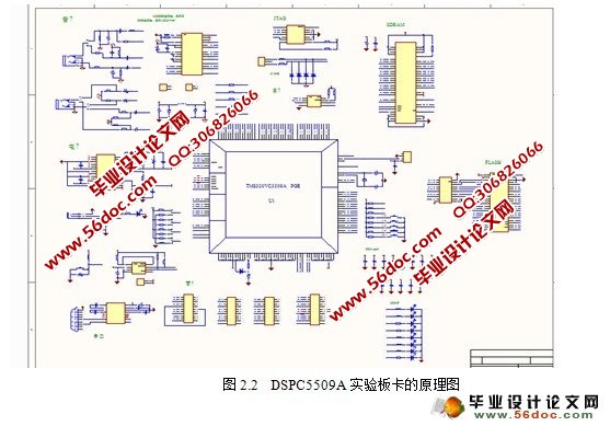
2.3 C5509A DSP实验板卡原理图设计 7
2.3.1 Altium Designer工具简介 7
2.3.2 电路原理图设计 7
2.3.3 电源模块 8
2.3.4 音频模块 11
2.2.5 异步串行通信MAX3232芯片 14
2.3.6 EEPROM存储 15
2.3.7 SDRAM 16
2.3.8 FLASH 17
第三章C5509A DSP的PCB设计及板卡的焊接 19
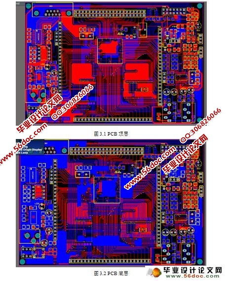
3.1 C5509A DSP实验板卡的PCB布线 19
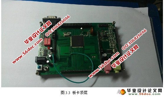
3.2 完成板卡的制作 21
第四章C5509A DSP实验板卡各功能模块的调试 24
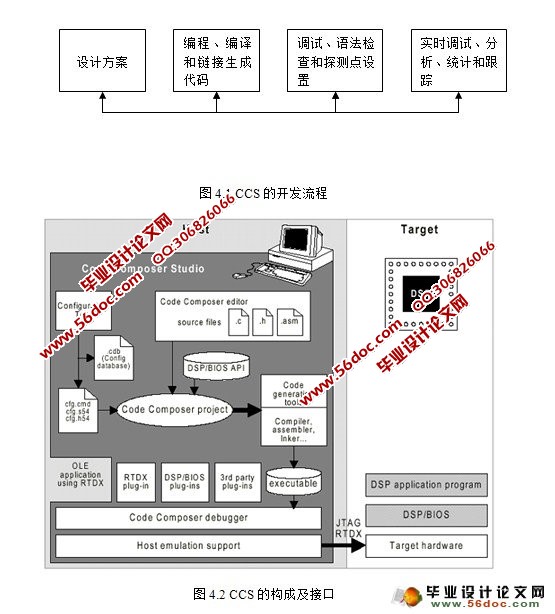
4.1开发工具及环境的介绍 24
4.1.1 CCS的构成介绍 24
4.1.2 CCS中文件的种类 25
4.1.3 CCS环境中的汇编/C语言程序开发 26
4.1.4 CCS中如何调试程序 28
4.2 结合CCS软件对PCB板卡的各功能模块进行调试。 29
4.2.1基于DSP最小系统的 FFT算法实现 30
4.2.2 数字信号处理FIR和IIR滤波器实验 32
总 结 36
参 考 文 献 37
致 谢 38