
光伏电源逆变器的设计(附PCB版图,电路原理图)
无需注册登录,支付后按照提示操作即可获取该资料.
光伏电源逆变器的设计(附PCB版图,电路原理图)(论文13400字,外文翻译)
摘 要
随着传统的三大化石能源日渐枯竭,绿色能源的开发和利用将会得到空前的发展,太阳能作为世界上最清洁的绿色能源之一,起并网发电备受世界各国普遍关注。而光伏并网发电系统的核心部件,如何可靠的高质量地向电网输送功率尤为重要,因此在可再生能源并网发电系统中起点能变换作用的逆变器成为了研究的一个热点。为此本文仍然采用“全桥逆变+LC滤波+工频升压”的逆变电源设计方案。整个系统设计分为SPWM波形产生电路、H桥驱动及逆变电路、欠压过流保护电路。
在SPWM波形产生环节,本文采用脉宽调制芯片SG3525的为核心。由文氏桥振荡电路产生50Hz的正弦波基准信号。然后经过精密整流、放大等处理输入到SG3525的补偿信号端,从而输出SPWM波。最后进行死区延时,输入到驱动电路中。
在驱动电路设计环节中,本文采用两片IR2110半桥驱动芯片构成全桥驱动电路。输出侧逆变电路中开关管选用耐压值高的MOSFET。然后经过工频变压器进行升压到市电,供家用电器使用。对输入、输出进行采样,实时监控是否欠压、过流,进行保护动作。
最后,给出额定功率为500W(输入电压12V输出交流220V)的单相逆变器样机的试验波形。
关键词:光伏电源,逆变器,SPWM,SG3525,IR2110
DESIGN OF PV POWER INVERTER
ABSTRACT
In recent years, photovoltaic technology has broad application. As our country's new energy law enacted, the photovoltaic power system in our country will have a broader space for development. Inverter is an important component in PV system. Its performance has great influence on the application of photovoltaic system. Currently, the domestic pure sine wave output inverter mainly uses 50Hz transformer for raising the output voltage, this paper is still developed an inverter by using the “Full-bridge circuit + LC filter + Isolator transformer” design proposal. The whole system is divided into SPWM waveform generator circuit, H bridge driver circuit and the inverter circuit, low voltage and over-current protection circuit.
In SPWM waveform generation part, this paper uses SG3525 PWM chip core. The Wien bridge oscillation circuit generates 50Hz sine reference signal. After this signal precision rectification, amplification and other processing of the compensation signal input to the SG3525-side, so this part output the SPWM wave. Finally, the SPWM signals enter into the driving circuit after dead-time delay.
In the design of drive circuit part, using two IR2110 half-bridge driver chips constitute a full-bridge driver circuit. The output side of inverter switch circuit selects high voltage value MOSFET. Then through 50Hz transformer, boost to the mains for household appliances. Testing the samples of the input and output voltage, real-time monitoring is under-voltage, over current, protection action.
Finally, rated power for 500W (Input voltage 12V, Output communication 220V) single-phase ac inverter prototype test waveforms have been given.
KEY WORDS: PV power, Inverter, SPWM, SG3525, IR2110
目 录
前 言 1
第1章 系统设计概述 3
§1.1 光伏电源逆变器的基本结构和设计要求 3
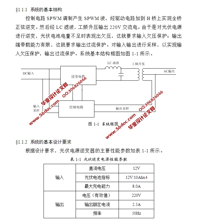
§1.1.1 系统的基本结构 3
§1.1.2 系统的基本设计要求 3
§1.2 系统电源设计 4
§1.3 逆变电路 4
§1.3.1 逆变电路的基本工作原理 4
§1.3.2 电压型逆变电路 5
§1.4 SPWM调制技术 6
§1.4.1 理论基础 6
§1.4.2 单极SPWM调制方式 7
§1.4.3 双极性SPWM调制方式 8
第2章 SPWM调制电路 9
§2.1 SG3525芯片介绍 9
§2.1.1 功能结构 9
§2.1.2 SG3525特性 10
§2.2 单极性SPWM调制电路 11
§2.2.1 SPWM调制电路结构 11
§2.2.2 正弦波发生器 12
§2.2.3 精密整流电路 14
§2.2.4 误差放大及加法电路 15
§2.2.5 SPWM调制 16
§2.2.6 时序控制电路 17
第3章 逆变电路 19
§3.1 IR2110芯片介绍 23
3.1.1功能结构 23
§3.1.2 IR2110特性 24
§3.2 驱动电路设计 26
§3.3 输出滤波器设计 27
§3.4 保护电路设计 29
第4章 系统调试 32
§4.1 信号板电路的调试 32
§4.2 信号板与H桥联调 34
§4.3 保护电路调试 36
结 论 37
参考文献 38
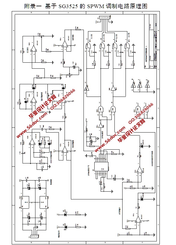
附 录 41